PCB Design & Development
Category: Electrical & Electronics
| Model | PCB Design & Development |
|---|---|
| Location | Nashik, India |
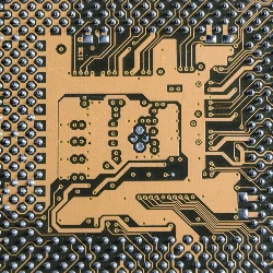
Product Description
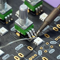
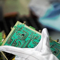
PCB Designing Services
Single Layer PCB Design
Double Layer PCB Design
Multilayer PCB Layout Design
Circuit Design and Development
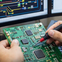
Schematic Design Services
PCB Prototype Development
Electronic Product Development Support
Single Layer PCB Design
Double Layer PCB Design
Multilayer PCB Layout Design
Circuit Design and Development
Schematic Design Services
PCB Prototype Development
Electronic Product Development Support

-
Address:
Saket, Parijat Nagar Signal (Mahatma Nagar),, Nashik, India - 422005
-
Business Hours:
9AM – 6PM
-
Working Days:
Monday Tuesday Wednesday Thursday Friday Saturday
-
Established:
2015